IR Camera Detector
Fanout Board
Printed
Circuit Board (pcb)
The
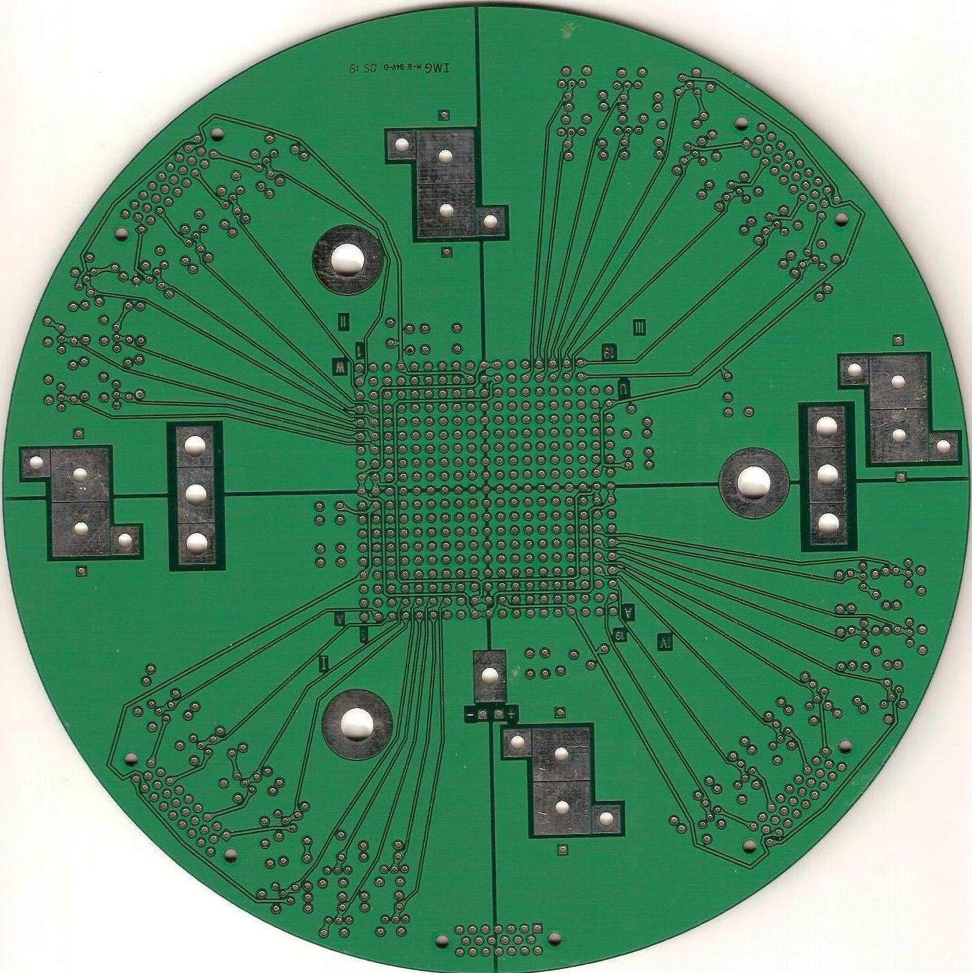
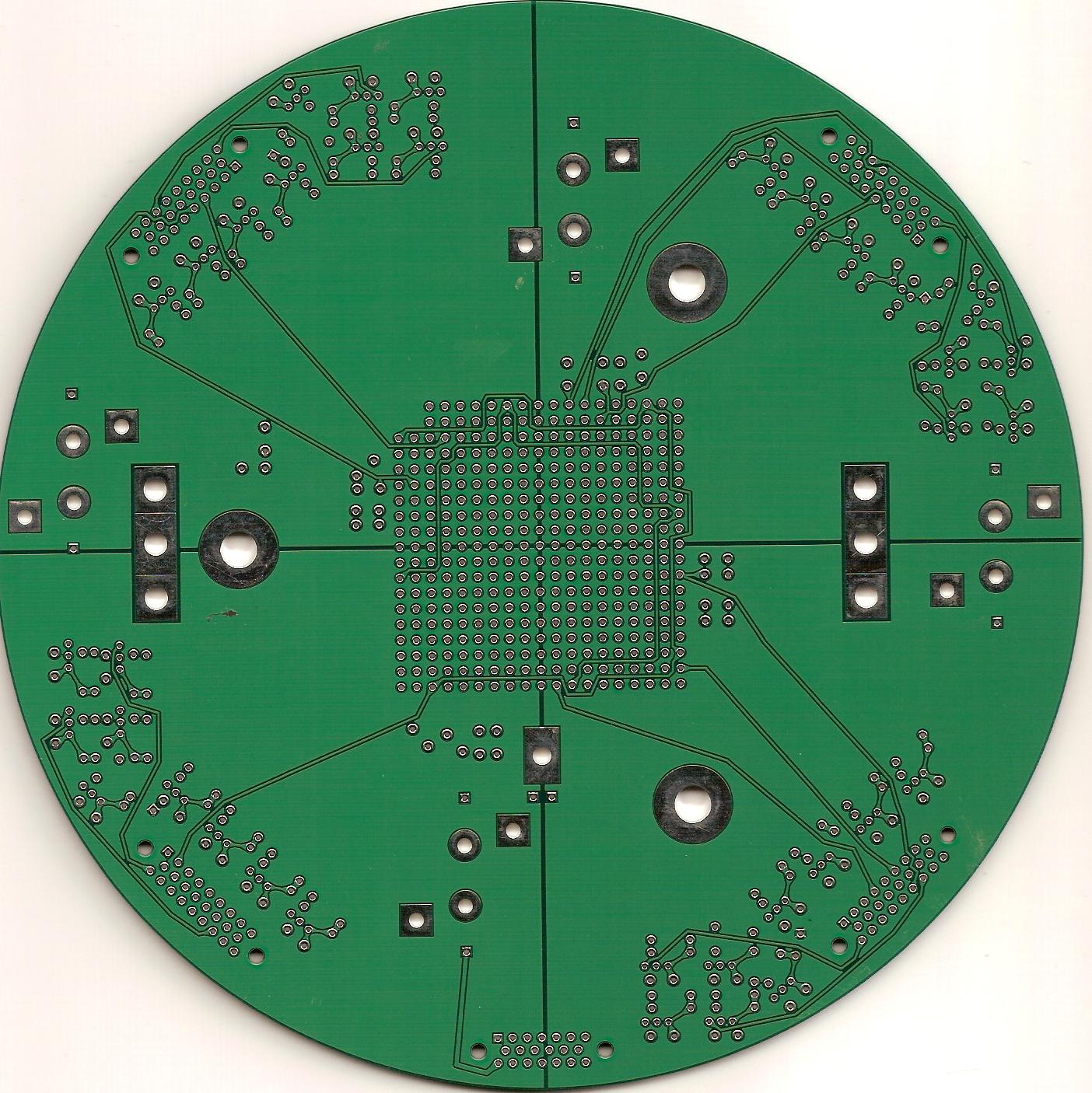
printed circuit board kindly provided by John Geary(CfA, Harvard).
The left image shows the 4 quadrants: I (lower left), II (upper
left), III (upper right) IV (lower right). The right image shows the
top of the pcb where the ziff socket will go(note the orientation of
the quadrants: I (lower right), II (upper right), III (upper left),
IV (lower left).
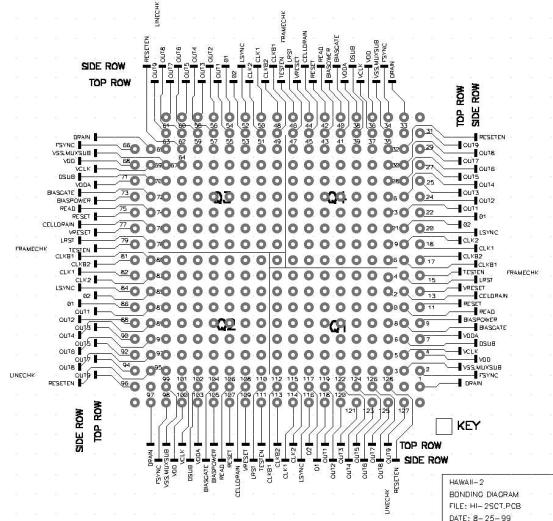
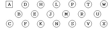
The pinout pattern of the 26 pin connector (Positronic SGM26FDS5T0000 / SGM26MDS5T000) as seen from the top of the pcb is shown below. Note the lettering begins with the square pin. The bonding pattern of the Hawaii-2 array was used to determine the pinout to the four 26 pin connectors on the pcb. An ohmmeter was used to trace the connections not visible on the multilayer pcb. Only 128 pins on the outer 2 rows are used for signals. The inner pins(221) are used for cooling the array and are coupled to the coldstrap mount points on the pcb.
Capacitors are used to filter the clock and bias signals. Specifically:(NIFS: http://www.mso.anu.edu.au/nifs/cdr/cdr-detector.htm)
100pF (100pF NPO Nickel Barrier Ceramic -55 to +125C, SMD1206) to filter the clocks. (4 ea.)
0.1uF (0.33uF FX7R Nickel Barrier Ceramic -55 to +125C, SMD1206) to filter the bias signals. Note the 0.33uF is expected to change to 0.1uF when at 77K. (4 ea.)
4.7uF (4.7uF Multicomp Tantalum, SMD size code B) is used to filter VRESET and BIASGATE (expected to drop to 3uF at 77K). (8 ea.)
Since the board provided has through holes for mounting components the surface mount components above are only listed as references to successful designs and will not necessarily be used. Surface mounting requires indium solder between the component and the surface of the board so as not to break with differential contraction when cooling to 77K. Components mounted by through hole have leads to provide the needed flexibility.
Buffer amplifiers are used on the outputs before leaving the pcb.
JFET LSK170A-92 (36 ea.)
capacitors TBD (36 ea.)
resistors TBD (2x36 ea.)
There are four locations designed for heater resistors which are controlled with the 20 pin connector as well as a temperature diode.
resistor TBD (4 ea.)
diode TBD (1 ea.)
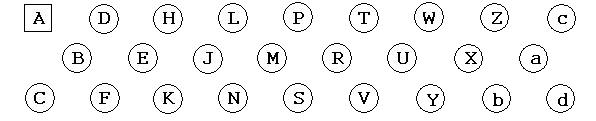
Below left is the pinout from the pcb to the 26 pin connectors for the clock, bias and output signals. Below right is the pinout from the pcb to the 20 pin connector for user signals(heaters, temperature sensors).
|
Pin |
I |
II |
III |
IV |
|
Pin |
|
|---|---|---|---|---|---|---|---|
|
A |
OUT5 |
OUT5 |
OUT5 |
OUT5 |
|
A |
|
|
B |
O2 |
O2 |
O2 |
O2 |
|
B |
|
|
C |
OUT2 |
OUT2 |
OUT2 |
OUT2 |
|
C |
HEATER |
|
D |
CLKB1,CLK2 |
O1 |
LSYNCH |
FSYNCH |
|
D |
|
|
E |
|
|
|
|
|
E |
|
|
F |
VDDA,BIASPOWER |
VDDA,BIASPOWER |
VDDA,BIASPOWER |
VDDA,BIASPOWER |
|
F |
|
|
H |
OUT8 |
OUT8 |
OUT8 |
OUT8 |
|
H |
+V, +I DIODE |
|
J |
VSS |
VSS |
VSS |
VSS |
|
J |
|
|
K |
OUT3 |
OUT3 |
OUT3 |
OUT3 |
|
K |
|
|
L |
CLKB2,CLK1 |
RESET |
RESETEN |
VCLK |
|
L |
|
|
M |
|
|
|
|
|
M |
|
|
N |
|
|
|
|
|
N |
|
|
P |
BIASGATE |
BIASGATE |
BIASGATE |
BIASGATE |
|
P |
-V,-I DIODE |
|
R |
MUXSUB |
MUXSUB |
MUXSUB |
MUXSUB |
|
R |
|
|
S |
OUT1 |
OUT1 |
OUT1 |
OUT1 |
|
S |
|
|
T |
DRAIN |
|
|
|
|
T |
|
|
U |
|
|
|
|
|
U |
|
|
V |
VRESET |
VRESET |
VRESET |
VRESET |
|
V |
|
|
W |
OUT7 |
OUT7 |
OUT7 |
OUT7 |
|
W |
|
|
X |
DSUB |
DSUB |
DSUB |
DSUB |
|
X |
HEATER |
|
Y |
OUT4 |
OUT4 |
OUT4 |
OUT4 |
|
|
|
|
Z |
|
|
|
|
|
|
|
|
a |
CELLDRAIN |
CELLDRAIN |
CELLDRAIN |
CELLDRAIN |
|
|
|
|
b |
VDD,LRST |
VDD,LRST |
VDD,LRST |
VDD,LRST |
|
|
|
|
c |
OUT9 |
OUT9 |
OUT9 |
OUT9 |
|
|
|
|
d |
OUT6 |
OUT6 |
OUT6 |
OUT6 |
|
|
|
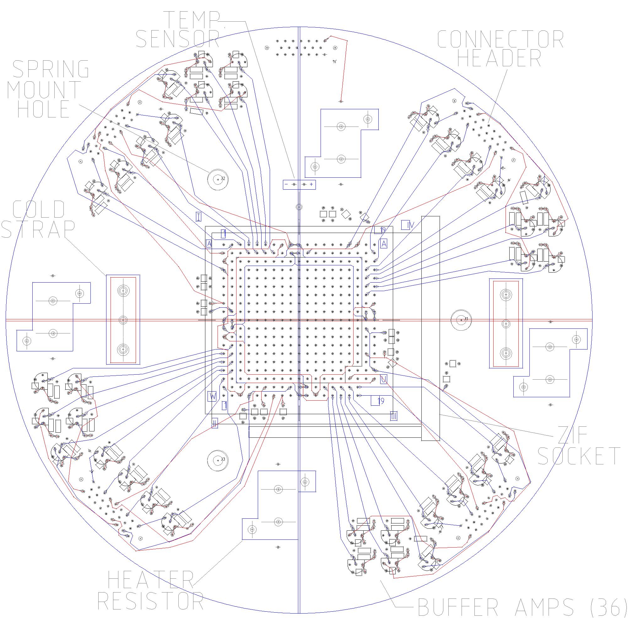
Below is a schematic (provided by John Geary) showing where the capacitors(squares), resistors(rectangles) and JFET's(semicircles) should be placed. Also shown is the Yamaichi NP89-44111-G4-BF ziff socket