|
Possible coexistence of magnetism and paramagnetic singularity in lightly Fe-doped WTe2Topological semimetals possess nodal or nodal-line phases where conduction and valence bands touch at points or lines in momentum space, respectively. Such band touching is symmetry protected and gives rise to exotic and interesting electronic properties. Coupling topological order with magnetism provides a platform for exploring time-reversal (TR) symmetry breaking topological physics, such as axion electrodynamics, inverse spin-galvanic effect, and the quantized anomalous Hall effect. The Weyl semimetal (WSM) requires breaking either TR symmetry or lattice inversion symmetry (I). By doping inversion-symmetry-broken WSM with magnetic dopants, one can expect to create a WSM with both symmetries breaking simultaneously. Here, structural, electrical, and magnetic properties of FexW1-xTe2 (x = 0 and 0.011) are reported. It is revealed that, with a small Fe doping concentration (x = 0.011), a ferromagnetism is induced at low temperature (<10 K). Scanning tunneling microscopy and spectroscopy measurements in Fe0.011W0.989Te2 further reveal only substitution and no intercalated dopants being observed. The probabilities of the Fe substitutions at the two nonequivalent W sites are quantified with equal probability. The dI/dV point spectra indicates that the Fe substitution in WTe2 manifests itself as electron doping regardless of doping sites. The results clearly reveal the possible coexistence of magnetism and Weyl points in the lightly Fe doped WTe2 at low temperature. This provides an ideal system for further study on the interplay between the topological Weyl points and the TR symmetry breaking. Read more: D. Baral et al., Phys. Rev. B 109, 245419 (2024). |
|
Tunneling current-controlled spin states in few-layer van der Waals magnetsEffective control of magnetic phases in two-dimensional magnets would constitute crucial progress in spintronics, holding great potential for future computing technologies. Here, we report a new approach of leveraging tunneling current as a tool for controlling spin states in CrI3. We reveal that a tunneling current can deterministically switch between spin-parallel and spin-antiparallel states in few-layer CrI3, depending on the polarity and amplitude of the current. We propose a mechanism involving nonequilibrium spin accumulation in the graphene electrodes in contact with the CrI3 layers. We further demonstrate tunneling current-tunable stochastic switching between multiple spin states of the CrI3 tunnel devices, which goes beyond conventional bi-stable stochastic magnetic tunnel junctions and has not been documented in two-dimensional magnets. Our findings not only address the existing knowledge gap concerning the influence of tunneling currents in controlling the magnetism in two-dimensional magnets, but also unlock possibilities for energy-efficient probabilistic and neuromorphic computing. Read more: Z. Fu et al., Nature Commun. 15, 3630 (2024). |
|
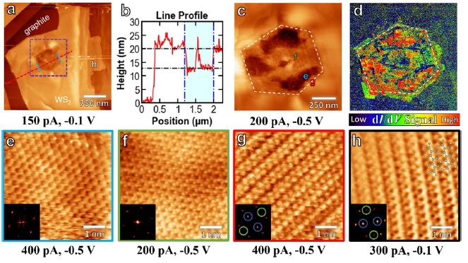
Local 2M (topological superconductor) to 2H (semiconductor) Phase Change in WS2The investigation of exotic properties in two-dimensional (2D) topological superconductors has garnered increasing attention in condensed matter physics, particularly for applications in topological qubits. Despite this interest, a reliable way of fabricating topological Josephson junctions (JJs) utilizing topological superconductors has yet to be demonstrated. Controllable structural phase transition presents a unique approach to achieving topological JJs in atomically thin 2D topological superconductors. In this work, we report the pioneering demonstration of a structural phase transition from the superconducting to the semiconducting phase in the 2D topological superconductor 2M-WS2. We reveal that the metastable 2M phase of WS2 remains stable in ambient conditions but transitions to the 2H phase when subjected to temperatures above 150 °C. We further locally induced the 2H phase within 2M-WS2 nanolayers using laser irradiation. Notably, the 2H phase region exhibits a hexagonal shape, and scanning tunneling microscopy uncovers an atomically sharp crystal structural transition between the 2H and 2M phase regions. Moreover, the 2M to 2H phase transition can be induced at the nanometer scale by a 200 kV electron beam. The electrical transport measurements further confirmed the superconductivity of the pristine 2M-WS2 and the semiconducting behavior of the laser-irradiated 2M-WS2. Our results establish a novel approach for controllable topological phase change in 2D topological superconductors, significantly impacting the development of atomically scaled planar topological JJs. Read more: S. Gautam et al., 2D Mater. 11, 015018 (2024). |
|
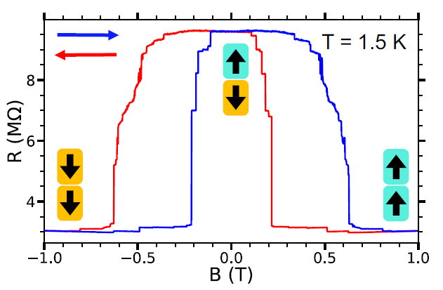
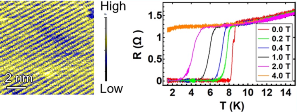
Two-Dimensional 2M-WS2 Nanolayers for SuperconductivityRecently, a newly discovered VIB group transition metal dichalcogenide (TMD) material, 2M-WS2, has attracted extensive attention due to its interesting physical properties such as topological superconductivity, nodeless superconductivity, and anisotropic Majorana bound states. However, the techniques to grow high-quality 2M-WS2 bulk crystals and the study of their physical properties at the nanometer scale are still limited. In this work, we report a new route to grow high-quality 2M-WS2 single crystals and the observation of superconductivity in its thin layers. The crystal structure of the as-grown 2M-WS2 crystals was determined by X-ray diffraction (XRD) and scanning tunneling microscopy (STM). The chemical composition of the 2M-WS2 crystals was determined by energy dispersive X-ray spectroscopy (EDS) analysis. At 77 K, we observed the spatial variation of the local tunneling conductance (dI/dV) of the 2M-WS2 thin flakes by scanning tunneling spectroscopy (STS). Our low temperature transport measurements demonstrate clear signatures of superconductivity of a 25 nm-thick 2M-WS2 flake with a critical temperature (TC) of ~8.5 K and an upper critical field of ~2.5 T at T = 1.5 K. Our work may pave new opportunities in studying the topological superconductivity at the atomic scale in simple 2D TMD materials. Read more: P. Samarawickrama et al., ACS Omega 6, 2966-2972 (2021). |
|
Small Energy Gap Revealed in CrBr3CrBr3 is a layered van der Waals (vdW) material with magnetic ordering down to the 2D limit. For decades, based on optical measurements, it is believed that the energy gap of CrBr3 is in the range of 1.68-2.1 eV. However, controversial results have indicated that the band gap of CrBr3 is possibly smaller than that. An unambiguous determination of the energy gap is critical to the correct interpretations of the experimental results of CrBr3. Here, we present the scanning tunneling microscopy and spectroscopy (STM/S) results of CrBr3 thin and thick flakes exfoliated onto highly ordered pyrolytic graphite (HOPG) surfaces and density functional theory (DFT) calculations to reveal the small energy gap (peak-to-peak energy gap to be 0.57 eV ± 0.04 eV; or the onset signal energy gap to be 0.29 ± 0.05 eV from dI/dV spectra). Atomic resolution topography images show the defect-free crystal structure and the dI/dV spectra exhibit multiple peak features measured at 77 K. The conduction band - valence band peak pairs in the multi-peak dI/dV spectrum agree very well with all reported optical transitions. STM topography images of mono- and bi-layer CrBr3 flakes exhibit edge degradation due to short air exposure (~15 min) during sample transfer. The unambiguously determined small energy gap settles the controversy and is the key in better understanding CrBr3 and similar materials. Read more: D. Baral et al., PhysChemChemPhys 23, 3225-3232 (2021). |
|
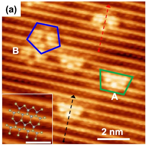
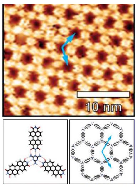
Hetero-molecular self-assembly with sub-5nm pore size on Graphene surfaceIn order to utilize the excellent electronic properties (high electron mobility), opening electron band gap for the gapless Graphene is highly desired. It has been demonstrated that to have applicable energy gap, graphene ribbons with width less than 10 nm is required. These graphene ribbons were mainly synthesized through top-down approaches, such as electron beam lithography. However, since graphene lattice has three-fold symmetry, the two dimensional ribbon structure has broken the symmetry of the graphene lattice, hence increase the scattering centers near the edge of graphene ribbons. To solve this problem, here, we adopted a bottom-up approach to modify graphene by means of non-covalent interactions on graphene surface. Two different organic molecules - PTCDI and melamine - have compatible structures to form directional hydrogen bonds. The resulting structure of the assemblies is hexagonal, same symmetry as the graphene. In addition to the non-covalent modification to graphene, the successful fabrication of the hexagonal assemblies could be further used as mask for subsequent stronger covalent modifications. Read more: H. J. Karmel et al., J. Phys. Chem. Lett. 5, 270 (2014). |
|
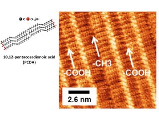
Sub-10 nm Templating for Atomic Layer Deposited Oxide on GrapheneSince the first successful isolation and transport measurement, graphene has been the focus of research. One of the reasons is that graphene has extraordinary high electron mobility for electronic applications. However, the gapless electronic structure makes graphene not ideal for making devices. In addition, chemically inert nature of graphene makes it even more difficult to handle. For example, the atomic layer deposition (ALD) growth of dielectric materials on graphene is suppressed. Here, we successfully utilized the ordered self-assembled chain-like organic molecules (10,12-pentacosadiynoic acid (PCDA)) as a template for oxide ALD growth. The grown oxide persist the line-like features and orders under controlled growth condition. This work paves the road to functionalize graphene for further modifications in nano-scale. Read more: J. M. P. Alaboson et al., Nano Lett. 13, 5763 (2013). |