|
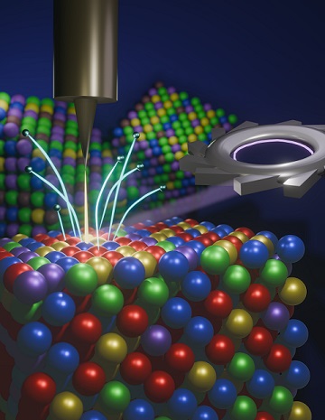
Distinguishing Elements at the Sub-Nanometer Scale on the Surface of a High Entropy AlloyMaterials in crystalline form possess translational symmetry (TS) when the unit cell is repeated in real space with long- and short-range orders. The periodic potential in the crystal regulates the electron wave function and results in unique band structures, which further define the physical properties of the materials. Amorphous materials lack TS due to the randomization of distances and arrangements between atoms, causing the electron wave function to lack a well-defined momentum. High entropy materials provide another way to break the TS by randomizing the potential strength at periodic atomic sites. The local elemental distribution has a great impact on physical properties in high entropy materials. It is critical to distinguish elements at the sub-nanometer scale to uncover the correlations between the elemental distribution and the material properties. Here, the use of synchrotron X-ray scanning tunneling microscopy (SX-STM) with sub-nm scale resolution in identifying elements on a high entropy alloy (HEA) surface is demonstrated. By examining the elementally sensitive X-ray absorption spectra with an STM tip to enhance the spatial resolution, the elemental distribution on an HEA's surface at a sub-nm scale is extracted. These results open a pathway towards quantitatively understanding high entropy materials and their material properties. Read more: L. Kim et al., Adv. Mater. 2402442 (2024). |
|
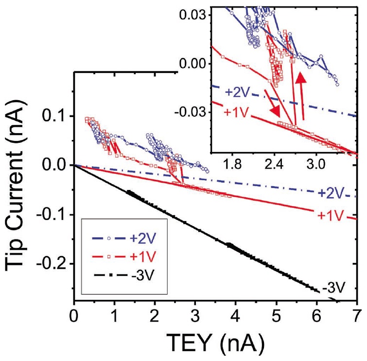
Fingerprinting of the Near to Far Field Transitions on Cu(111) Surface Induced by Synchrotron RadiationThe combining of the high spatial resolution of scanning tunneling microscopy (STM) with chemical and magnetic contrast provided by synchrotron X-ray has the unique characterization capability for novel materials. Traditional STM electronics only monitor tip current to gain information of topography and electronic local density of states, based on the fact that the tip current is the same as the sample current. However, when combining STM with synchrotron X-ray, photo-ejected electrons from sample or tip may escape from tip-sample system, resulting tip current and sample current are not the same. Furthermore, while the STM electronics under constant tip current mode for topographic scanning, this tip current contains both tunneling current and photo-current simultaneously. In other words, when the photo-current is equal to or larger than the current set-point, the z-piezo, which control the tip-sample distance, will retract the tip out of tunneling region and lost information. Here, unlike traditional STM system, we monitored both the tip current and sample current simultaneously and determined the fingerprint of the far field (out of tunneling region). Read more: V. Rose et al., Adv. Funct. Mater. 23, 2646 (2013). |
|
Spin-Dependent Synchrotron X-ray Excitations Probed with Scanning Tunneling MicroscopyX-ray magnetic linear dichroism (XMLD) and x-ray magnetic circular dichroism (XMCD) are two modes of the synchrotron x-ray spectroscopy that reveal the orientation of charge distribution and the magnetic moment near the targeted ions, respectively. The spatial resolution of the traditional XMLD and XMCD is in micro-meter scale, which is limited by the spot size of the synchrotron x-rays. Recent developments in nano-probing techniques are targeting to shrink the spot size. An alternative approach is to change the probing mechanism. By using SXSTM, the photo-ejected electrons by illuminating synchrotron x-rays are collected by a special prepared smart tip (see below). Here, we demonstrate that by switching the left circularly polarized (LCP) and right circularly polarized (RCP) synchrotron x-rays in the SXSTM system, the XMCD signal could be probed by the smart tip. This demonstration pushes the spatial resolution of XMCD by alternating the probing method. Read more: V. Rose et al., J. Appl. Phys. 111, 07E304 (2012). |
|
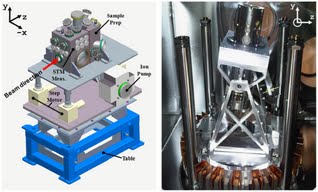
Combining Synchrotron X-ray with Scanning Tunneling Microscopy (SXSTM)Combining a scanning tunneling microscopy (STM) with synchrotron X-ray beamline provides a novel way of studying materials with excellent spatial resolution and element sensitivity. Special designed tilting stage on the damping platform allows the X-ray incident angle adjustment. The UHV chamber, where STM houses, sits on a massive platform, which reduces noisy environment of synchrotron endstation. Tunable horizontal and vertical positions of the whole platform enable the alignment of X-ray to the tip-sample junction. Read more: M.L. Cummings et al., Ultramicroscopy 112, 22 (2012). |
|
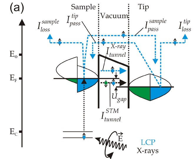
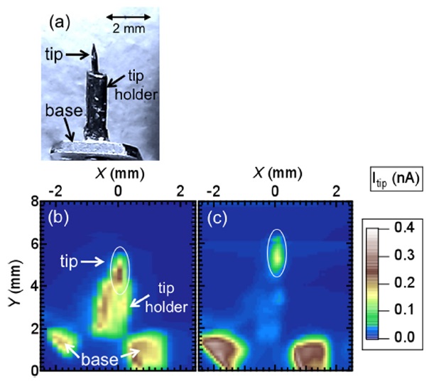
Smart tip for SXSTMIn order to develop an instrument with atomic spatial resolution and ability of element sensitivity, we combined the synchrotron x-ray and the scanning tunneling microscopy (STM). Traditional STM works under the assistant of the quantum tunneling effect when brought a metallic, atomically sharp tip to the vicinity of conductive sample surfaces. When illuminating synchrotron x-ray onto the tip-sample junction simultaneously, photo-ejected and photo-induced electrons could be detected and/or excited and collected by the metallic tip. However, the photo-ejected electrons collected by side walls of the tip will degrade the spatial resolution. In order to solve this problem, a smart tip is needed. A smart tip is a metallic tip, Pt90Ir10 tip in this case, coated with insulating material, SiO2 in this case, but with the apex of the tip opened for collecting tunneling and photo-ejected electrons. Nano-tomography revealed the detail coating situation near the tip apex. The photoemission mappings of the tips, coated and bare, show the reducing signal effect from the tip side walls due to the insulating materials. This type of smart tip would be ideal for SXSTM measurement. Read more: V. Rose et al., Appl. Phys. Lett. 99, 173102 (2011). |