
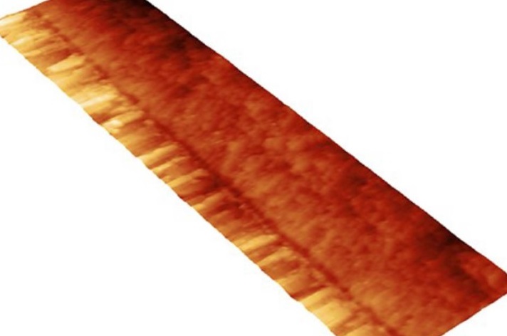
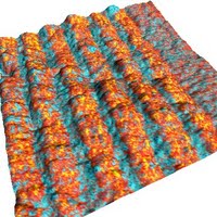
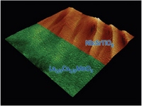
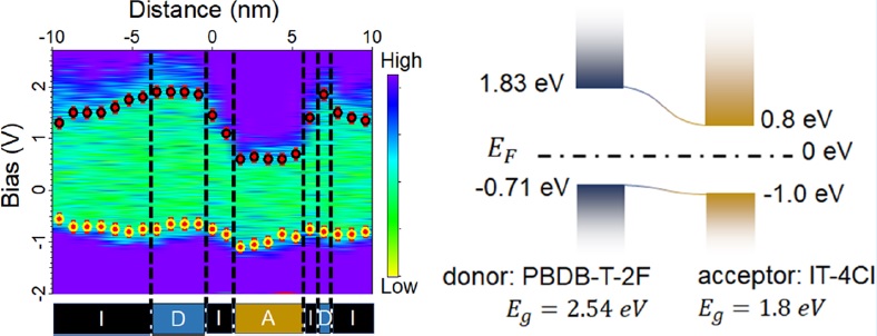
Cross-Sectional Scanning Tunneling Microscopy/Spectroscopy (XSTM/S) on Complex Oxides
Interfaces have been utilized in semiconductor industry for providing electronic devices for decades. Recent studies on complex oxide materials revealed much more variety of functionalities in one type of materials. Epitaxially grown complex oxide interfaces further demonstrated novel physical phenomena unseen in the composite substrates and films. Due to the highly interacting environment (charge, lattice, spin and orbital coupling), the understanding of the complex oxides and the interfaces is limited. Existing experimental techniques for studying complex oxide interfaces would either provide excellent spatial resolution without capability of showing physical properties or probing physics properties without atomic resolutions. The cross-sectional scanning tunneling microscopy and spectroscopy (XSTM/S) for complex oxide interfaces is recently developed in our lab. With this technique, the local electronic density of states near the interfaces could be spatially mapped out with atomic resolutions. Read more.
 |
 |
 |
 |
 |
 |
 |
Electron-Phonon Coupling on Be(0001)
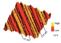
Many-body interactions in condensed matter physics is becoming very important when the materials of interests are moving toward more functional materials. In addition, in low-dimensional materials, the many-body interactions are strongly deviating from their bulk counterparts. To study this complex interactions in low-dimensional environment, we focused on the electron-phonon coupling on the Be(0001) surfaces. By using angle-resolved photoemission spectroscopy (ARPES), the behavior of the surface electrons are measured and detail analysis is conducted. The electron-phonon coupling on Be(0001) surfaces is revealed surprisingly to be anisotropic on the isotropic Fermi contour of surface electrons. This anisotropy was also found to be the origin of the long reported controversial measured electron-phonon coupling strength: mass-enhancement factor. Further detail study was conductive with extremely high quality ARPES and determined detail contributions from surface phonon modes and bulk phonon modes on the electron-phonon coupling on the surfaces. These works provide a pathway for studying more complicated many-body interactions in low-dimensional environments. Read more.
 |
 |
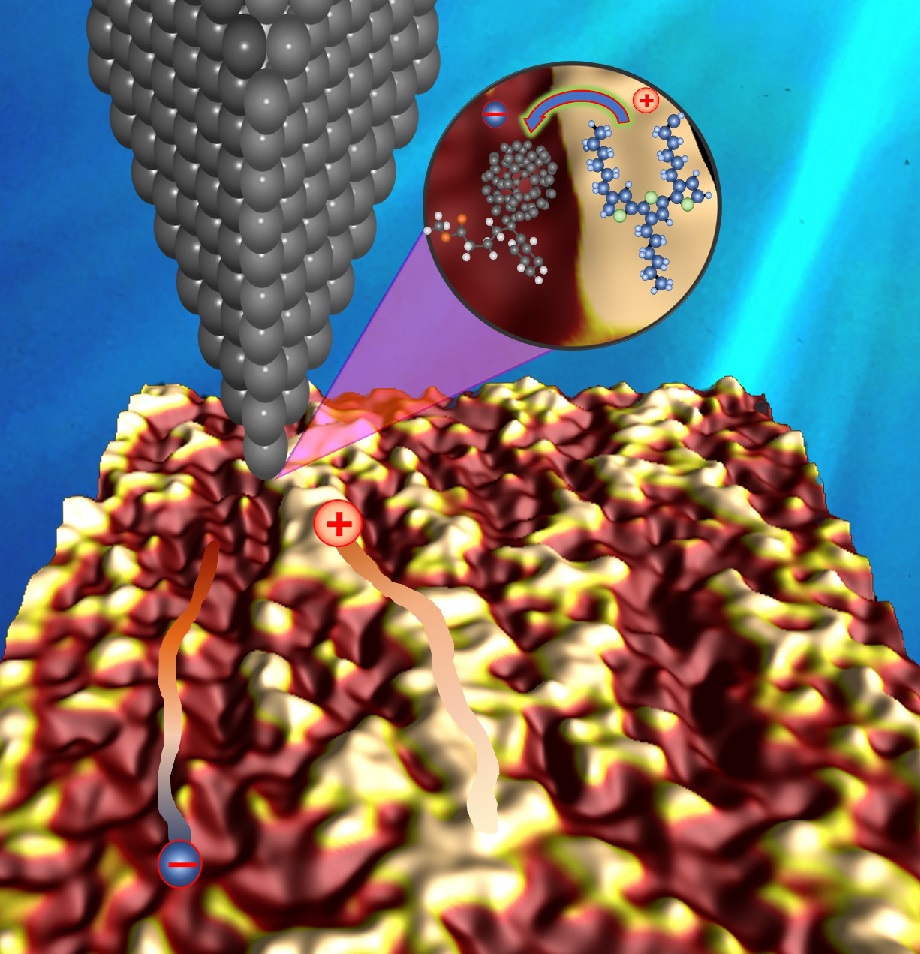
Solar Cell Materials
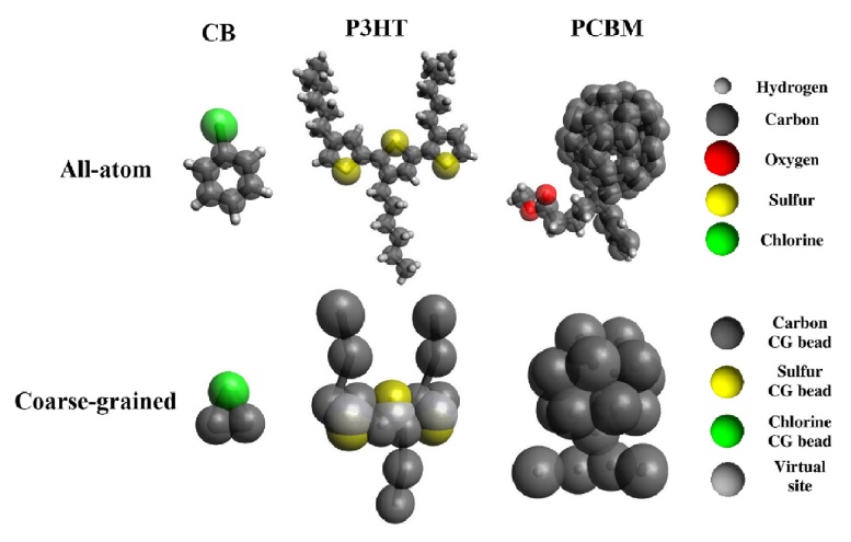
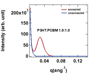
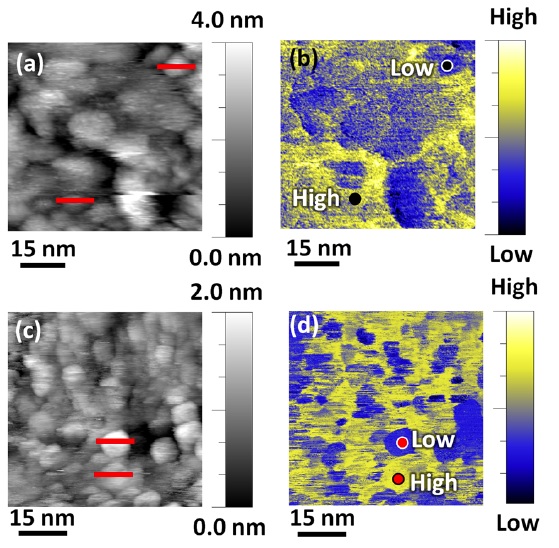
Renewable energy resources are explored widely to seek strategies to replace fossil fuel comsumption. Photovotaic materials and devices are one of the major developing renewable energy technology aim to convert the photon emitted by the Sun into electricity. Among various types of developing photovoltaic materials and devices, quantum-dot sensitized solar cell (QDSSC), organic photovoltaic cell (OPVC) and organometallic halide perovskite based solar cell (PSC) hold high hope for revolutionize the photovoltaic applications. In our group, we have done studies about the materials used in QDSSC, in OPVC, and in PSC to seek fundamental and microscopic understanding of their working principles. With these knowledge, we anticipate to provide unique information to guide researchers and engineers routes to design next generation solar cells. Read more.
 |
 |
 |
 |
 |
 |
 |
 |
 |
 |
 |
 |
 |
 |
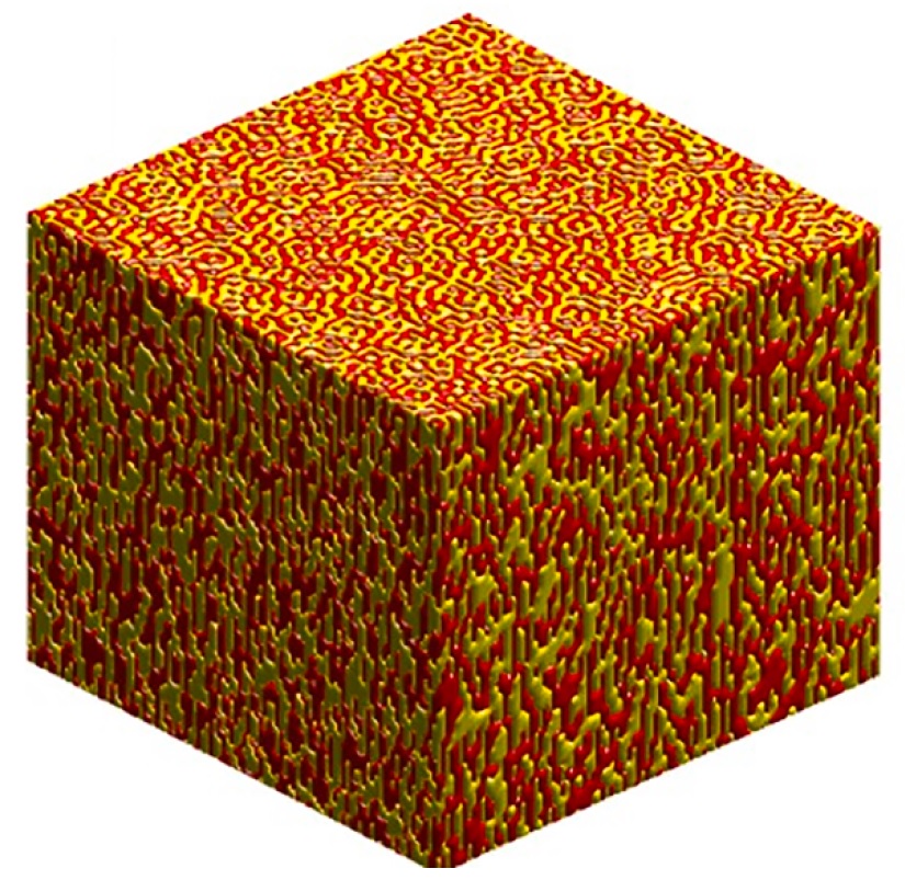
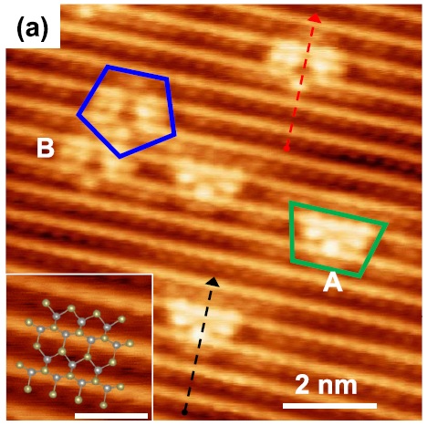
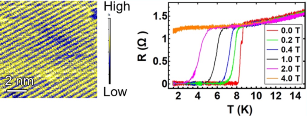
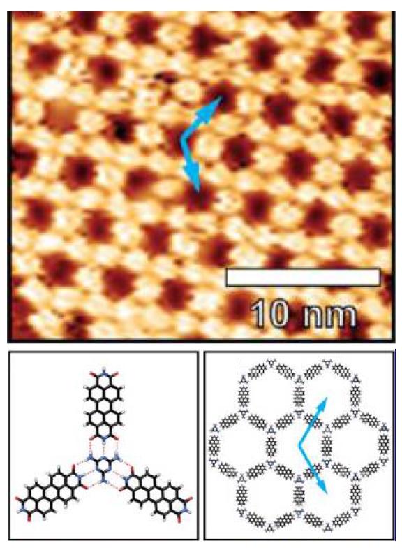
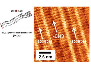
2D vdW Materials
Since the first isolation in 2004, graphene has drawn plenty of attention in scientific community, and was awarded the Nobel Prize for the ignition of the graphene research frenzy. This intense interest further extented toward other materials and now developed into a whole family of 2D van der Waals (vdW) materials. We have studied various 2D materials using scanning tunneling microscopy and spectroscopy (STM/S). The materials of interests are topological superconductors, 2D magnets, and molecular self assemblies. Read more.
 |
 |
 |
 |
 |
 |
 |
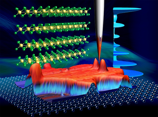
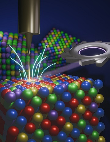
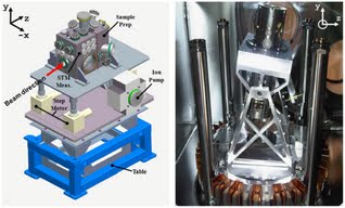
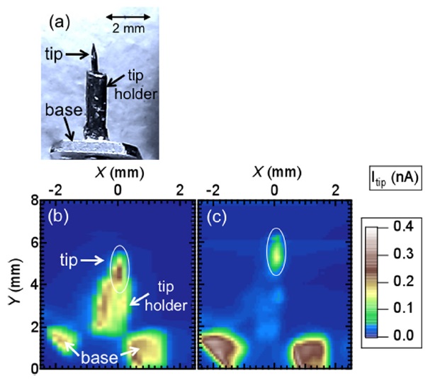
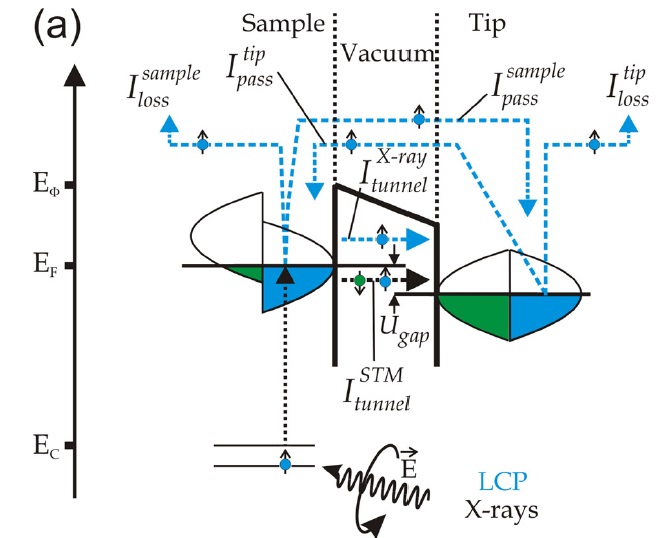
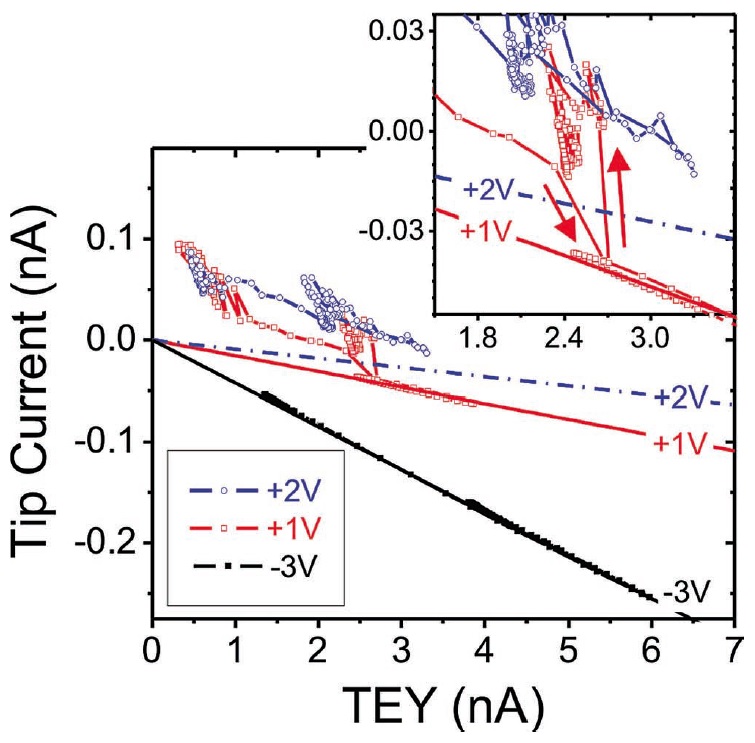
Synchrotron X-ray Scanning Tunneling Microscopy (SXSTM)
One of the goals in nanoscience is to develop an instrument with both atomic resolution and chemical element sensitivity. By combining the scanning tunneling microscopy (STM), which has excellent spatial resolution, with synchrotron X-ray, which has chemical element sensitivity, this goal is expected to be achieved. In order to reduce the background signal due to the photoelectrons collected by the side wall of the STM tip, insulator coating on the STM tip is needed. In addition to the chemical element sensitivity, the SXSTM could potentially provide magnetic moment information in nano-scale by using X-ray magnetic circular dichroism (XMCD) mode with coated STM tip. Read more.
 |
 |
 |
 |
 |
Catalytic Materials
Catalytic materials are one of the foundations for the modern society. Chemical reactions can be manipulated with the catalytic processes for economical benefit. Understanding the catalytic materials at nanoscale will provide great insights in designing and improving them. We utilize scanning tunneling microscopy (STM) to study these materials in collaborations with catalysis experts on this directions Read more.
 |
 |
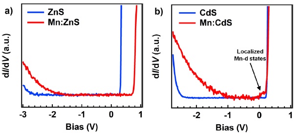
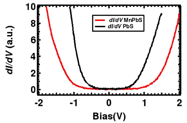
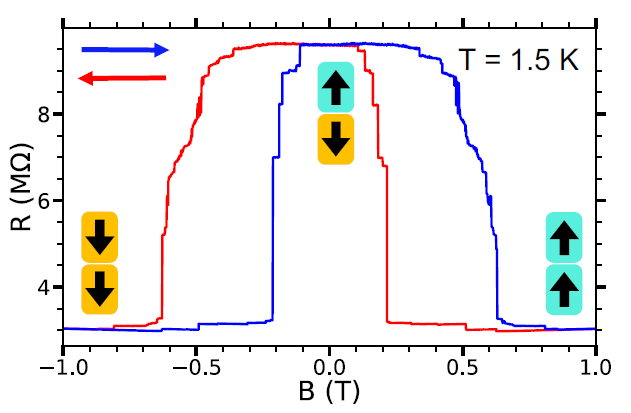
Magnetic Materials
Magnetic materials are functional materials with plenty of applications, including information handling. By utilizing scanning tunneling microscopy (STM) and spin-polarized STM, a various magnetic materials and their nm-scale properties are studied. Read more.
 |
 |
|
|
|
 |
|
|
|
|
|
|
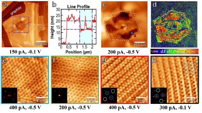
Quantum Materials
Quantum materials provide platform for quantum phenomena control. It has tremendous applications in quantum information science and engineering. By using STM, we focus on revealing quantum state properties of various types quantum materials. Read more.
|
|
|
|
|
|
|
|
|
|
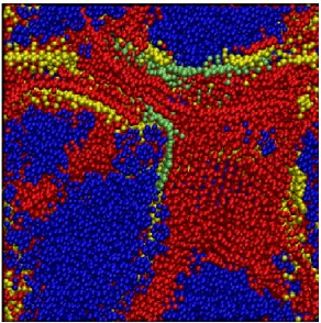
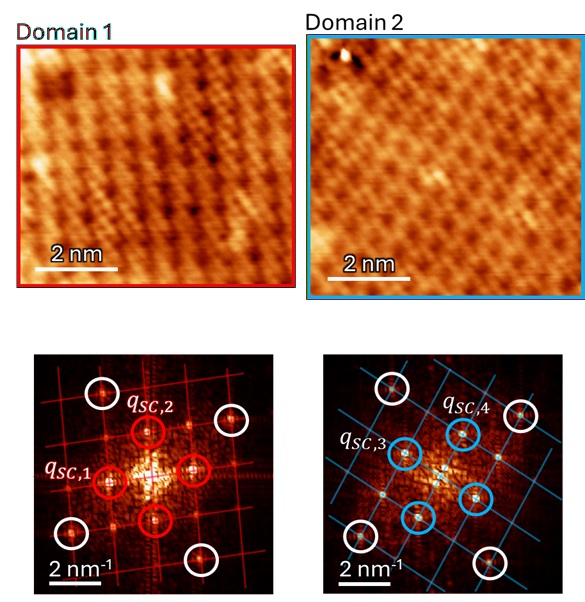
Direct visualization of the existence of surface local chemical order in a high-entropy CoCrFeMnNi alloyThe impacts of local chemical order (LCO) on the physical properties of high-entropy alloys (HEAs) have been widely discussed. However, the difficulty in unambiguously observing LCO with high precision poses a great challenge in establishing microscopic mechanisms regarding the impacts of LCO on physical properties. Furthermore, it is still unclear whether the LCO extends to HEA surfaces, which may impact surface-based properties, such as corrosion, oxidation, and catalytic activities. Through the utilization of scanning tunneling microscopy (STM), two surface LCO domains with corresponding √5 x √5 R ± 26.6 ° quasi-long-range orderings (QLRO) are directly observed on a CoCrFeMnNi surface. Density functional theory (DFT) calculations identify the LCO within QLRO supercells. The findings provide evidence of the existence of the surface LCO and demonstrate a method to directly observe the surface LCO of HEAs. With the ability to unambiguously resolve elemental configuration at atomic scale, the understanding of how LCO influences surface-based properties can be achieved, facilitating the design of HEAs with tailored functionalities. Read more: Kim et al. Nature Comm. https://doi.org/10.1038/s41467-026-71170-z. |
|
Converting raw coal powder into polycrystalline nano-graphite by metal-assisted microwave treatmentA metal-assisted microwave treatment that converting raw coal powders into nano-graphite is presented. Specifically, four major factors are identified for successful conversion: (1) high temperature; (2) reducing environment; (3) catalyst; and (4) microwave radiation. Specifically, it is determined that the combination of the carbon sources (raw coal powders), the high temperature (microwave induced electric sparking), the reducing environment (the Ar/H2 mixture), the catalyst (Cu foil), with the microwave radiations can generate nano-graphites. This novel approach utilizes the sparking induced by the microwave radiation on the fork-shape metal foils to generate high temperature (> 1000 °C) within a few seconds. The small thermal load makes this method cost effective and has potential for higher temperature using metals with higher melting temperature. Refinement of this technique is possible to yield a higher quality and quantity of nano-graphite materials for a wider range of applications. Read more: Masi et al. Nano-Structures & Nano-Objects 25, 100660 (2021). |
|
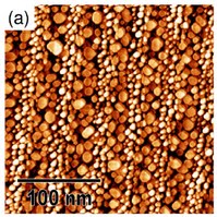
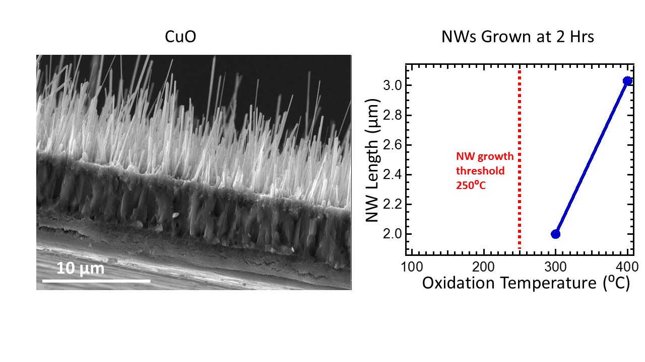
Controlled Growth of Copper Oxide Nano-WiresCopper oxide has been used for various applications such as gas sensors, capacitors, and solar cells. Copper oxide grows in two stoichiometric forms, CuO and Cu2O. CuO can be grown in various nano forms including nanoparticles, films, flowers, and wires. Using the direct oxidization method on the pure Cu foils, we have recently found that the threshold temperature and duration for the growth of CuO nanowires (NWs) through direct oxidation is 250 °C for 2 hrs. Using Raman Spectroscopy, X-ray Diffraction (XRD), and Scanning Electron Microscopy (SEM) we have found clear evidence that a Cu2O layer forms prior to the growth of CuO NWs. Our research has also shown that at low oxidation temperatures (250 °C - 400 °C), the lengths and widths of the NWs increased with oxidation duration and temperature while previous studies at temperatures above 400 °C showed the width decreasing with increasing temperature. Our data and findings help to clarify the growth process of CuO NWs. Read more: J. Hilman et al., Nano-Structures Nano-Objects 11, 124-128 (2017). |
|
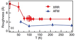
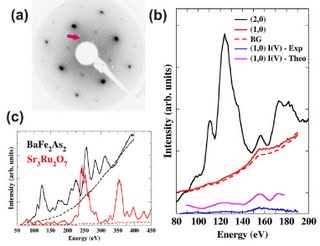
Determination of the Surface Termination of Cleaved BaFe2As2Iron-based superconductors (pnictides) have drawn plenty attentions recently, since the discovery of their high critical superconducting temperatures (Tc). The major reason is these type of materials provide a whole new arena for testing the high-Tc superconductivity theory, which was solely built with information from copper-based superconductors (cuprates). Since many tools, such as angle-resolved photoemission spectroscopy (ARPES) and scanning tunneling microscopy (STM), used to understand the microscopic phenomena of superconductivity are surface sensitive, the understanding of the surface termination/structure is very important to interpret the data took by surface sensitive tools. We combined the low energy electron diffraction (LEED) intensity vs beam energy (I-V) curves analysis and STM data to determine the surface terminations of the cleaved BaFe2As2(001) surface. Read more: V.B. Nascimento et al., Phys. Rev. Lett. 103, 076104 (2009). |
|
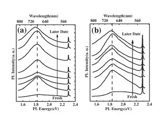
Photoluminescence of Nano-Crystalline Si Enclosed in Oxidized ShellSilicon (Si) is one of the most studied material and widely used in semiconductor industry due to its unique properties. The indirect band gap of Si has limited it to the devices manipulating electrons only, but not the photons - the exiton recombination efficiency is low. Recent studies showed that the efficiency of the light emission due to exiton recombination could be dramatically enhanced in nano-scaled Si. Possible mechanisms of the enhancement have been proposed and could be sorted into (1) quantum confinement for exitons in the nano particles; (2) the recombination centers located at the interfaces. In our lab, we synthesized different sizes of Si Quantum Dots (QDs) and characterize its photoluminescence (PL) signal as function of the time aged after exposed to air. We conclude that, in our Si QDs, the recombination centers at interfaces between the nano-crystalline Si core and the oxidized shell is responsible the enhanced exiton recombination process. Read more: (1) TeYu Chien et al., Chinese J. Phys. 46, 91 (2008); (2) TeYu Chien et al., Int. J. Nanosci. 2, 357 (2003). |
|
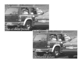
Restoration of the Out-of-focus PicturesOut-of-focus pictures are commonly seen in many regular camera usages. Sometimes the out-of-focus pictures could cause severe problems, such as the pictures taken by the surveillance system. Hardware upgraded system could partially solve this problem, but costly. In our lab, we developed a software-based solution, which can be installed in the already exist surveillance system to deal with the out-of-focus pictures with the help of Fourier Transform Algorithm. This method could have further usage to many scientific measurements with resolution issues, and thus reduce the demands for the developments for the higher resolution instruments, which usually cost a great amount of R&D funds. Read more: C.-H. Chen et al., Innovative Comput., Inf. and Control Express Lett. 2, 409 (2008). |